- 您现在的位置:买卖IC网 > Sheet目录472 > MAX2140EVKIT (Maxim Integrated)EVAL KIT MAX2140
�� �
�
�Complete� SDARS� Receiver�
�ABSOLUTE� MAXIMUM� RATINGS�
�V� CC_XX� to� GND.....................................................� -0.3V� to� +4.3V�
�VINANT� to� GND....................................................� -0.3V� to� +5.6V�
�AGCPWM� to� GND� ................................................� -0.3V� to� +3.0V�
�Digital� Input� Current� ........................................................� ±10mA�
�Maximum� VSWR� Without� Damage� ........................................� 4:1�
�Maximum� VSWR� Without� Oscillations� ...................................� 4:1�
�All� Other� Pins� ...............................................� -0.3V� to� V� CC� +� 0.3V�
�Continuous� Power� Dissipation� (T� A� =� +70°C)�
�44-Pin� TQFN� (derate� 26.31mW/°C� above� +70°C)� ...� 2105mW�
�Operating� Temperature� Range� ..........................-40°C� to� +85°C�
�Junction� Temperature� .....................................................+150°C�
�Theta� J� C� ..........................................................................12°C/W�
�Storage� Temperature� Range� ............................-65°C� to� +150°C�
�Lead� Temperature� (soldering,� 10s)� ................................+300°C�
�Stresses� beyond� those� listed� under� “Absolute� Maximum� Ratings”� may� cause� permanent� damage� to� the� device.� These� are� stress� ratings� only,� and� functional�
�operation� of� the� device� at� these� or� any� other� conditions� beyond� those� indicated� in� the� operational� sections� of� the� specifications� is� not� implied.� Exposure� to�
�absolute� maximum� rating� conditions� for� extended� periods� may� affect� device� reliability.�
�CAUTION!� ESD� SENSITIVE� DEVICE�
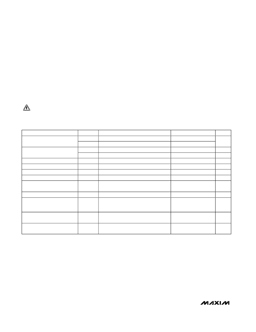
�DC� ELECTRICAL� CHARACTERISTICS�
�(V� CC� =� 3.1V� to� 3.6V;� VINANT� ≥� V� CC� ,� VOUTANT� in� open� circuit,� T� A� =� -40°C� to� +85°C.� Typical� values� are� at� V� CC� =� 3.3V,� VINANT� =�
�3.3V,� and� T� A� =� +25°C,� unless� otherwise� noted.)� (Note� 1)�
�PARAMETER�
�SYMBOL�
�CONDITIONS�
�MIN�
�TYP�
�MAX�
�UNITS�
�Supply� Voltage� Range� (Note� 2)�
�Operating� Supply� Current�
�V� CC�
�VINANT�
�I� CC�
�I� SHDN�
�All� blocks� on�
�All� blocks� off�
�3.1�
�3.1�
�3.3�
�3.3�
�150�
�30�
�3.6�
�5.3�
�180�
�V�
�mA�
�μA�
�Lock� Indicator� High� (Locked)�
�Lock� Indicator� Low� (Unlocked)�
�Digital� Input-Logic� High�
�Digital� Input-Logic� Low�
�V� IH_LK�
�V� IL_LK�
�V� IH�
�V� IL�
�V� CC� -� 0.5�
�V� CC� -� 0.5�
�0.5�
�0.5�
�V�
�V�
�V�
�V�
�Input� Current� for� Digital� Control�
�Pins�
�Input� Current� for� AGCPWM�
�Voltage� Drop� VINANT� to�
�VOUTANT� in� Normal� Operating�
�Mode�
�I� DIG�
�I� AGCPWM�
�V� ANTDC-�
�DROP�
�Maximum� current� sink� at� VOUTANT� is�
�150mA�
�-1�
�-10�
�+1�
�+290�
�0.35�
�μA�
�μA�
�V�
�Current� Sink� at� VOUTANT� to� Flag�
�Bit� ACP� =� 1�
�I� ANTDC_H�
�VOUTANT� shorted� to� ground� (Note� 4)�
�195�
�500�
�mA�
�Current� Sink� at� VOUTANT� to� Flag�
�Bit� AND� =� 1�
�I� ANTDC_L�
�12�
�20�
�30�
�mA�
�2�
�_______________________________________________________________________________________�
�发布紧急采购,3分钟左右您将得到回复。
相关PDF资料
MAX2150ETI+T
IC MODULATOR I/Q WIDE 28TQFN
MAX2160EVKIT
EVAL KIT MAX2160
MAX2163ETI/V+
IC TUNER ISDB-T LOW IF 28TQFN
MAX2165EVKIT+
KIT EVAL FOR MAX2165
MAX2170EVKIT+
KIT EVAL FOR MAX2170
MAX2202EWT+T
IC POWER DETECTOR RMS 6-WLP
MAX2203EWT+T
IC RMS PWR DETECTOR 6WLP
MAX2204EVKIT+
KIT EVAL FOR MAX2204
相关代理商/技术参数
MAX2141ETH/V+
功能描述:射频接收器 XM Satellite Radio Receiver RoHS:否 制造商:Skyworks Solutions, Inc. 类型:GPS Receiver 封装 / 箱体:QFN-24 工作频率:4.092 MHz 工作电源电压:3.3 V 封装:Reel
MAX2141ETH/V+T
功能描述:射频接收器 XM Satellite Radio Receiver RoHS:否 制造商:Skyworks Solutions, Inc. 类型:GPS Receiver 封装 / 箱体:QFN-24 工作频率:4.092 MHz 工作电源电压:3.3 V 封装:Reel
MAX2141ETH+
功能描述:射频接收器 XM Satellite Radio Receiver RoHS:否 制造商:Skyworks Solutions, Inc. 类型:GPS Receiver 封装 / 箱体:QFN-24 工作频率:4.092 MHz 工作电源电压:3.3 V 封装:Reel
MAX2141ETH+T
功能描述:射频接收器 XM Satellite Radio Receiver RoHS:否 制造商:Skyworks Solutions, Inc. 类型:GPS Receiver 封装 / 箱体:QFN-24 工作频率:4.092 MHz 工作电源电压:3.3 V 封装:Reel
MAX2141EVKIT
制造商:Maxim Integrated Products 功能描述:EVAL KIT - Boxed Product (Development Kits)
MAX214C/D
功能描述:RS-232接口集成电路 RoHS:否 制造商:Exar 数据速率:52 Mbps 工作电源电压:5 V 电源电流:300 mA 工作温度范围:- 40 C to + 85 C 安装风格:SMD/SMT 封装 / 箱体:LQFP-100 封装:
MAX214CPI
功能描述:RS-232接口集成电路 Integrated Circuits (ICs) RoHS:否 制造商:Exar 数据速率:52 Mbps 工作电源电压:5 V 电源电流:300 mA 工作温度范围:- 40 C to + 85 C 安装风格:SMD/SMT 封装 / 箱体:LQFP-100 封装:
MAX214CPI+
功能描述:RS-232接口集成电路 Prog DTE/DCE 5V RS232 Transceiver RoHS:否 制造商:Exar 数据速率:52 Mbps 工作电源电压:5 V 电源电流:300 mA 工作温度范围:- 40 C to + 85 C 安装风格:SMD/SMT 封装 / 箱体:LQFP-100 封装: